DIODE
Diode only blocks current in the reverse direction while the reverse voltage is within a limited range otherwise reverse barrier breaks and the diode only blocks current in the reverse direction while the reverse voltage is within a limited range otherwise reverse barrier breaks and the voltage at which this breakdown occurs is called reverse breakdown voltage. The diode acts as a valve in the electronic and electrical circuits. A PN junction is the simplest form of the semiconductor diode which behaves as ideally short circuit when it is in forward biased and behaves as ideally open circuit when it is in the reverse biased. Beside simple PN junction diodes, there are different types of diodes although the fundamental principles are more or less same. So a particular arrangement of diodes can convert AC to pulsating DC, and hence, it is sometimes also called as a rectifier. The name diode is derived from "di - ode" which means a device having two electrodes.Symbol of Diode
The symbol of a diode is shown below. The arrowhead points in the direction of conventional current flow. We can create a simple PN junction diode by doping donor impurity in one portion and acceptor impurity in other portion of silicon or germanium crystal block. These dopings make a PN junction at the middle part of the block beside which one portion becomes p-type (doped with trivalent or acceptor impurity), and another portion becomes n-type (doped with pentavalent or donor impurity). We can also form a PN junction by joining a p-type (intrinsic semiconductor doped with a trivalent impurity) and n-type semiconductor (intrinsic semiconductor doped with a pentavalent impurity) together with a special fabrication technique. Hence, it is a device with two elements, the p-type forms anode, and the n-type forms the cathode. These terminals are brought out to make the external connections.
Working Principle of Diode
Unbiased Diode
N-side will have a significant number of free electrons, and very few holes (due to thermal excitation) whereas the p side will have a high concentration of holes and very few free electrons. Due to this, a process called diffusion takes place. In this process free electrons from n side will diffuse (spread) into the p side and recombine with holes present there, leaving positive immobile (not moveable) ions in n side and creating negative immobile ions in the p-type side of the diode.oltage at which this breakdown occurs is called reverse breakdown voltage. The diode acts as a valve in the electronic and electrical circuits. A PN junction is the simplest form of the semiconductor diode which behaves as ideally short circuit when it is in forward biased and behaves as ideally open circuit when it is in the reverse biased. Beside simple PN junction diodes, there are different types of diodes although the fundamental principles are more or less same. So a particular arrangement of diodes can convert AC to pulsating DC, and hence, it is sometimes also called as a rectifier. The name diode is derived from "di - ode" which means a device having two electrodes.Symbol of DIODE
The symbol of a diode is shown below. The arrowhead points in the direction of conventional current flow.
We can create a simple PN junction diode by doping donor impurity in one portion and acceptor impurity in other portion of silicon or germanium crystal block. These dopings make a PN junction at the middle part of the block beside which one portion becomes p-type (doped with trivalent or acceptor impurity), and another portion becomes n-type (doped with pentavalent or donor impurity). We can also form a PN junction by joining a p-type (intrinsic semiconductor doped with a trivalent impurity) and n-type semiconductor (intrinsic semiconductor doped with a pentavalent impurity) together with a special fabrication technique. Hence, it is a device with two elements, the p-type forms anode, and the n-type forms the cathode. These terminals are brought out to make the external connections.

Working Principle of Diode
Unbiased Diode
N-side will have a significant number of free electrons, and very few holes (due to thermal excitation) whereas the p side will have a high concentration of holes and very few free electrons. Due to this, a process called diffusion takes place. In this process free electrons from n side will diffuse (spread) into the p side and recombine with holes present there, leaving positive immobile (not moveable) ions in n side and creating negative immobile ions in the p-type side of the diode.Testing of diode
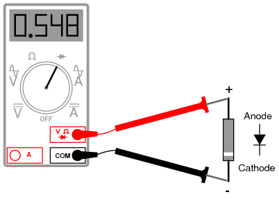

Meter with a “Diode check” function displays the forward voltage drop of 0.548 volts instead of a low resistance.

Determination of diode polarity: (a) Low resistance indicates forward bias, black lead is cathode and red lead anode (for most meters) (b) Reversing leads shows high resistance indicating reverse bias.
No comments:
Post a Comment